Printed Circuit Boards design has long defied automation, but could an AI-assisted workflow help alter the paradigm for optimising the process? LUKE VASSALLO seems to think so, and he’s dedicating his master’s degree to it.

Electronic circuit boards give anything electronic the ability to fulfil its promise, and that is true whether we’re talking about mobile phones or washing machines. Yet the process of creating printed circuit boards (PCBs) is a complex one that, so far, must be done pretty much manually from beginning to end. Luke Vassallo’s master’s is looking at how this could be fixed.
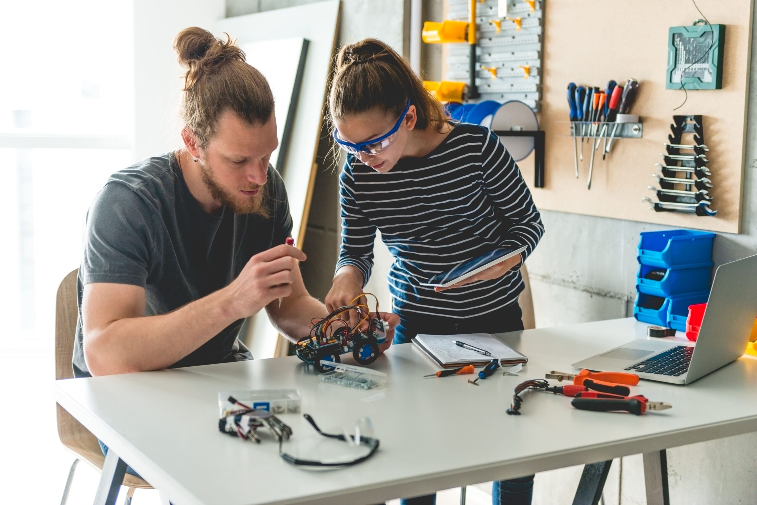
“PCBs are basically 3D, multi-layered structures that provide a surface for soldering on integrated circuits and multiple internals layers for running the interconnecting wires,” explains Luke, who is now a full-time master’s student following a stint as a Digital Signal Processing Engineer, which saw him designing the internal systems for dynamic positions of vessels out at sea.
“At all levels, these electronic circuit boards are complex to design and, even in an age of automation, the chips still must be placed and routed by hand, making it a time-consuming process which only specialists can do.”
It’s with this in mind that Luke decided to combine two disciplines to figure out a way of developing an AI tool to assist PCB designers by automating large parts of the design process.
The first is electronic design automation (EDA), which refers to a field dedicated to developing tools essential to modern electronic design. These help design, develop, and test complex circuits like integrated circuits and PCBs. In a nutshell, these allow engineers to be productive by enabling the computer to manage a part of the process that would be otherwise impossible for humans to do.
The second is Reinforcement Learning (RL). This sees a type of artificially-intelligent agent autonomously learn through trial-and-error interaction with its environment. By framing the PCB design problem in this setting, the agent tries different practices and receives ‘rewards’ when it gets things right and ‘punishments’ when it doesn’t, helping it build an understanding of what works.
“After learning the process, we asked the system to optimise several circuits that were derived from real-world projects, such as analogue sensor interfaces, mixed-signal circuitry, and digital subsystems such as dataloggers.”
“It learnt to do an excellent job that is similar to that performed by a human engineer”
Luke’s main contribution to this project, which is being worked on together with his supervisors, was to see whether the system would actually learn how to place chips on the PCB boards. As he explains, their observation was that, once the system learnt the fundamental dynamics of the problem, it did an excellent job that is similar to that performed by a human engineer.
This could now greatly assist specialists working on the process, while simultaneously reduce the cost of creating PCB. This is especially so when considering the fact that a user would not know whether a PCB would work until it has been manufactured, which often leads to much toing and froing between the design/hardware team and the manufacturing companies that create such PCBs.
“At this point, this project is still in its prototype phase, but we are advancing,” Luke continues. “In the future, I see two main users for it: hobbyists and people who are interested in technology but lack the strong background to design advanced circuit boards. In fact, there are many who like to experiment with circuit boards just for fun or to automate all sorts of stuff around their homes, such as building as clever gadgets, home automation devices, and weather stations.”
Asked why he feels it’s important to create this, Luke replies that such a project would be giving power to people who don’t have technical knowledge on PCBs. Yet, as he himself admits, this project could also help professionals, as it could be used to accelerate the design process for actual circuit designers, resulting in fewer and faster design cycles. This shows that such projects come with a lot of promise that could go beyond the boundaries of the University.