This work presents an implementation of a direct digital synthesis (DDS) system, on both a software level and a hardware level. Such systems could be implemented on devices such as sound synthesisers and function generators. DDS is a signal-processing technique that combines digital and analogue methods, in order to produce an arbitrary waveform while using a fixed-reference clock. The use of digital methods permits the DDS synthesiser to operate over a wide range of frequencies, extending to the megahertz (MHz) range. This is possible due to its capability of fast frequency hopping.
In order to change the output frequency of a DDS system, a procedure known as the phase-accumulator method was used. The phase accumulator relies heavily on a component called the binary tuning word (BTW). In essence, the BTW is the value by which the phase accumulator increases. The phase values were then portrayed as wave outputs by using a phase-to-amplitude convertor. The fundamental waveform associated with DDS is the sine wave, as seen in this project. DDS popularity is constantly on the rise, due to its high frequency capabilities. Consequently, its use in industry is also on the increase.
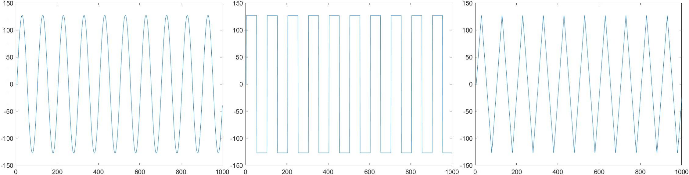
The objective of this project was to implement a DDS system onto a field-programmable gate array (FPGA), the implementation of which also entailed simulations taking place on a software level. The DDS system was implemented for 3 types of waves: sine, square and triangular. The algorithm was first implemented as a prototype on MATLAB and the resultant plots were deemed correct upon verification. The hardware implementation, written in the VHDL programming language, consisted of 2 parts, namely: the VHDL simulation itself and the running of the VHDL code on a hardware level by using an FPGA.
By simulating the VHDL code, it was noted that the DDS system was verified to work for frequencies from 10kHz to 5MHz. However, due to limitations brought about by the FPGA connectors, only the lowest frequency from the range (i.e., 10kHz) was outputted on the oscilloscope. This limitation was only present when the code was running on the FPGA, and the output values were directly generated. More importantly, if the DDS system was to be used as one stage in a larger FPGA project, this limitation would not impact the output.
Lastly, in order to carry out the final hardware implementation, a digital-to-analogue convertor (DAC) was used. Its role was to convert the digital signal outputted by the FPGA into an analogue waveform. This analogue wave was then passed through a filter which was used to create a smooth and clear wave on the oscilloscope display.
Course: B.Sc. (Hons.) Computer Engineering
Supervisor: Dr Ing. Trevor Spiteri